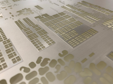
The Multilevel Screens are designed to print
more than one height in a single pass and
deposit the necessary paste for the different components of the circuit.
This is achieved by making a recess on the spatula side of the Stencil. It is also used more and more to save areas of the PCB such as graphite, silver bridges or via true hole and to achieve a good contact of the Stencil with the PCB. In this case, the recess is made on the PCB side of the Stencil.


There are various manufacturing processes to obtain the different heights in the Stencils for SMD:
Chemical etching
A chemical etching process is used to lower the material in certain areas
thus achieving different levels on each side of the Stencil.
It is not recommended to make recesses of greater than 100 microns, to ensure good
rugosity and thickness tolerance.
Thickness tolerance of +/- 10 microns.
Dimensional recess tolerance of +/- 150 microns.
Machining – CNC
This is a high-precision machining process to lower the material in
certain areas and achieve different levels on both sides of the stencil.
This process allows a ramp to be obtained between the different levels to facilitate the application of the
Rebates can be greater than 100 microns without compromising material roughness or
thickness tolerance.
Thickness tolerance of +/- 5 microns.
Dimensional recess tolerance of +/- 100 microns.
Laser spot welding
This is performed by welding two sheets of material, one on top of the other, using a
laser to achieve the desired height on both sides of the stencil.
The added material must be finer than the base material to achieve a good result in the
welding and the final flatness of the stencil.
Thickness tolerance of +/- 5 microns.
Dimensional recess tolerance of +/- 50 microns.

